DipTrace offers different prices for different packages [1]. The cheapest version, DipTrace Starter (300 pins, 2 signal layers), is available for $ 75. DipTrace Full offers unlimited pins and unlimited signal layers for $ 895. All versions of DipTrace come with a humongous parts library and 3D models for a large amount of general purpose parts. In case a part or footprint is not included in the libraries, DipTrace offers both a component editor and a pattern editor for custom parts.
I needed a super small PCB for 78XX type voltage regulators. This mini project was perfect for my first steps with DipTrace. Please be aware that this article is going to be extremely coarse as it is supposed to be a general overview of the DipTrace software. The functionality of this software is rather complex as this is a professional design tool. More detailed articles will follow.
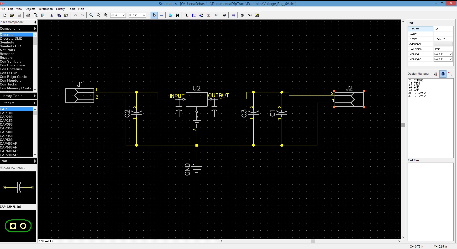
DipTrace Schematic Overview
The starting point for my project was the “Schematic Capture” module. It looks very neat and very well ordered. The positioning of all toolbars and elements seems very intuitive. I selected a 78XX voltage regulator, 1 shunt capacitor for the input side and 2 shunt capacitors for the output. I like to put a small capacitor (~ 100 nF) and a larger capacitor (~10 μF) on the output of my linear regulator circuits. Additionally I put a screw terminal each on the input and output side. It took less than 5 minutes to get the circuit together. To be fair, I totally forgot to enter component values in the schematic capture as I was rushing through it.
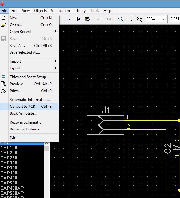
Convert to PCB
After the schematic is complete, the next step is to convert it to a PCB layout. The parts library links schematic symbols and PCB footprints. So when you click on “Convert to PCB”, the layout will be pre-loaded with the right footprints for the selected parts.
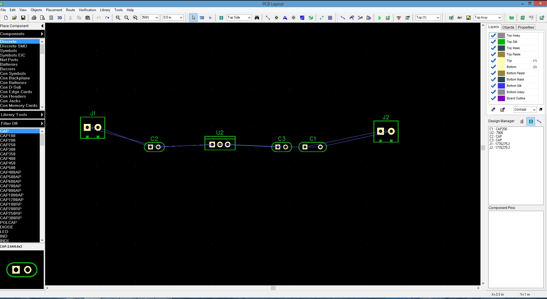
Initial Conversion View
The initial part placement is of course anything else than ideal. Although it seems that DipTrace’s PCB layout module tries to place the parts the same way they were input in the schematic capture. A keyboard shortcut for rotating parts “Ctrl + R” makes it easy to place the parts in the correct location. If you would like to manually route your PCB from this point on, you can do so. But the more comfortable way is to feed the autorouter with design rules and let it suggest a layout. If you don’t define a board outline beforehand, the autorouter will actually take care of that. In my case I selected a board outline beforehand and then let the autorouter run. It actually created a very usable layout. Nonetheless I fine-tuned the layout manually. After that I placed a copper pour on the bottom layer of the PCB. One setting for the copper pour, the Net it gets connected to, is hidden away and I totally oversaw it at first. As a result, my copper pur wasn’t connected to ground. I had to go back and set the pour to be connected to Net 0 in the “Connectivity” tab.
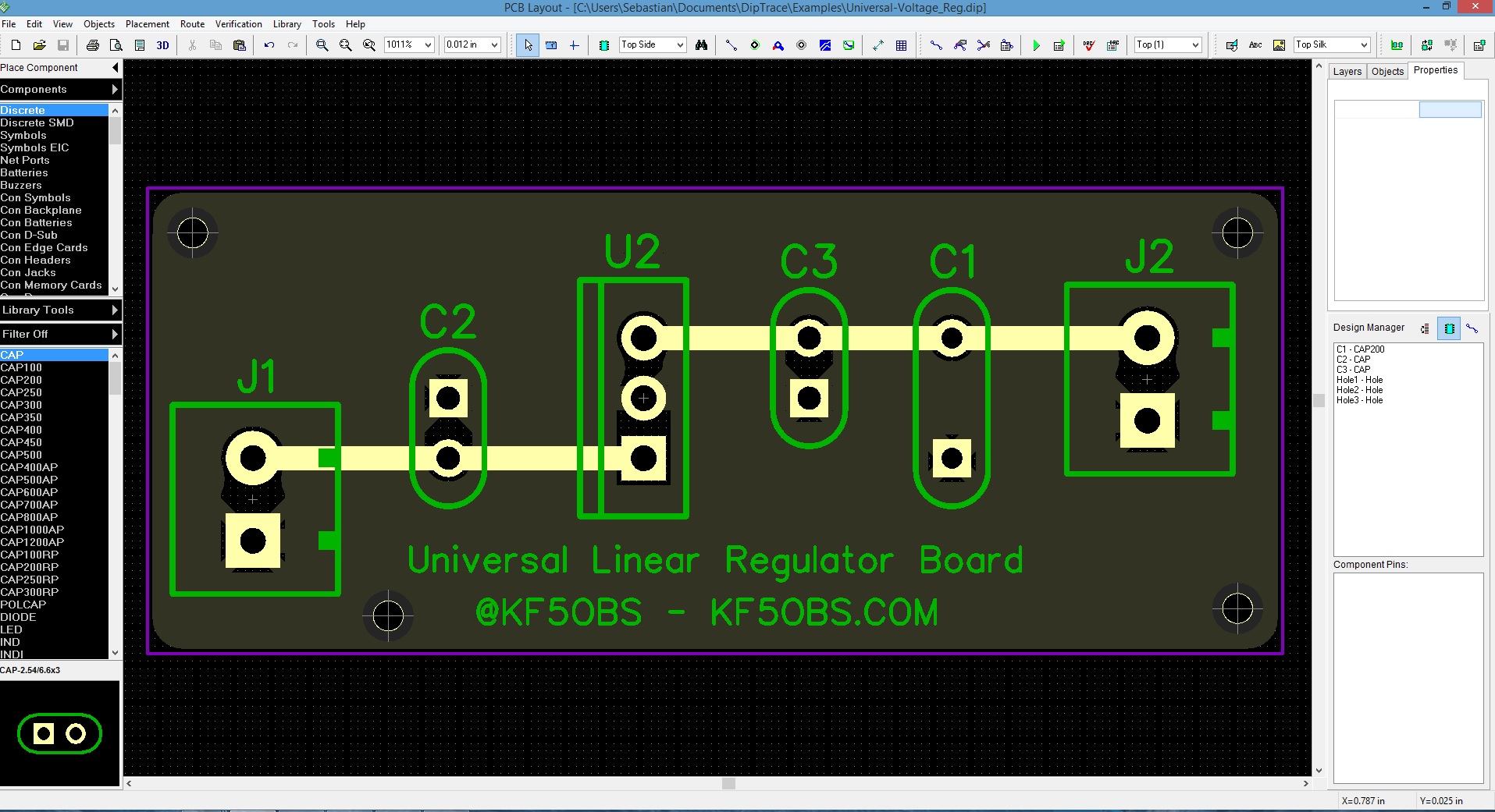
Finished PCB Layout
After The final design is completed, DipTrace offers a 3D preview of the board. This is a very nice feature for collision avoidance and to detect physical spacing problems between parts early in the design stage. You’d be surprised how often it happens even win professional designs that some clearance issue renders a PCB revision useless. So make deliberate use of the 3D modelling if 3D layouts are available for the parts you are using.
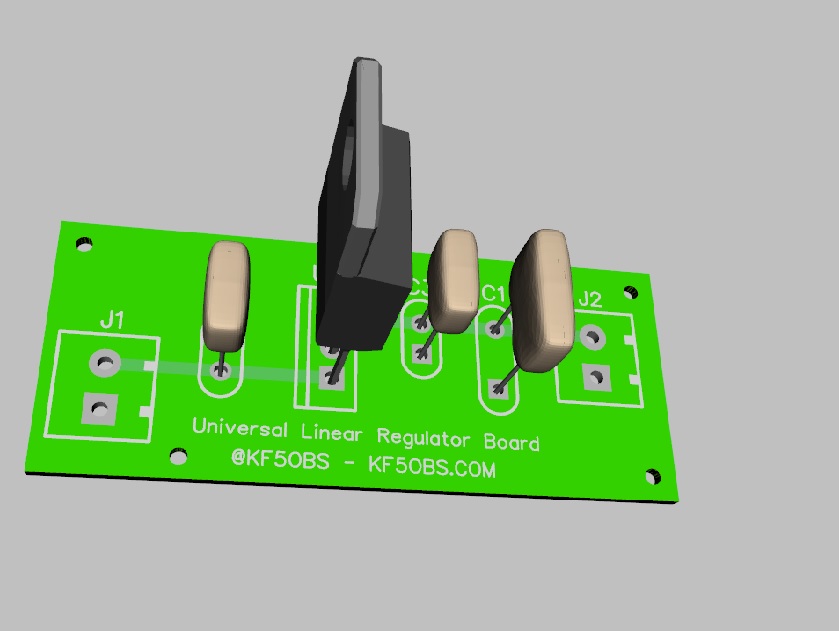
3D render of the PCB
The 3D part library is very large but DipTrace of course offers the option to upload custom 3D models as industry standard .wrl files. If everything goes well through this step, it’s time to get the PCB to the PCb manufacturer. DipTrace actually has an inbuilt “Order PCB” function.

BayArea Circuits Order Menu
The inbuilt “Order PCB” function is a service offered through BayArea PCB. As the name suggests, it’s a California based fabrication house [2]. Unfortunately, they don’t offer any options, just a standard 1.6 mm thick FR4 board with silk screen on both sides and HASL finish is offered. But the prices are more than fair for a US based manufacturer. 25 PCBs of my design cost $ 3 each or $ 75 total for instance.
But that’s not the fabrication house I wanted to use. For a long time I wanted to try the services of Dirty PCBs ([3]). Dirty PCB sends your order off to various Chinese fabrication houses, depending on what kind of board (e.g. 2-layer or 4-layer) you are submitting. They promise an ultra low-profile system with minimum customer service and options but extremely low, unbeatable prices. But more about them in a different article, let’s get back to the layout export.
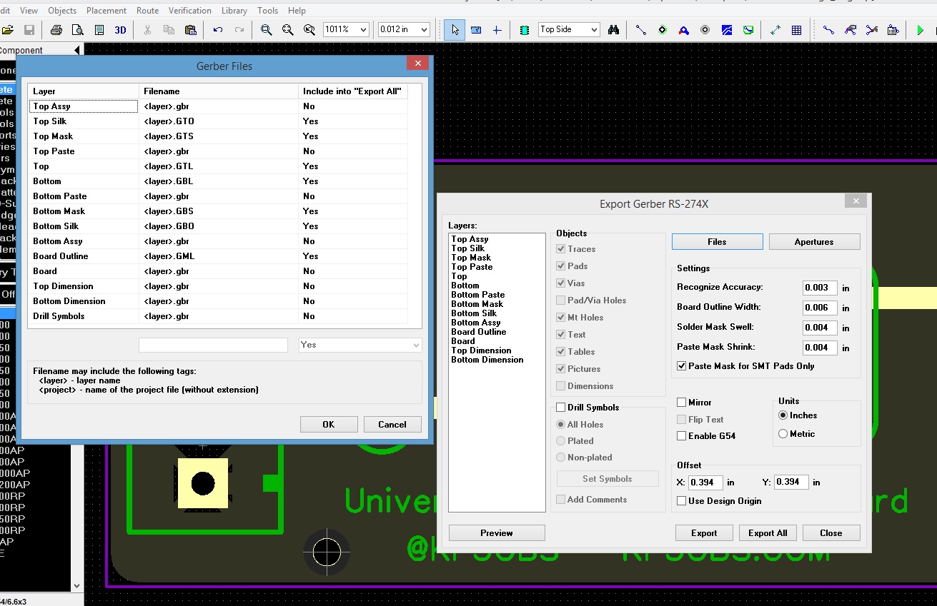
Correct Gerber Nomenclature for Dirty PCB
The de facto industry standard for exporting PCB layouts are Gerber files. Different PCB manufacturers use different naming schemes for Gerber files. Some expect the Gerber files to have a specific name, others expect any name but with a specific extension per layer and some want both. Make sure you know the exact specifications for your PCB manufacturer. The above is the correct extension nomenclature for Dirty PCBs.
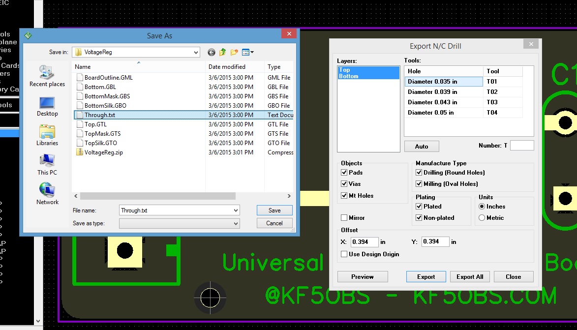
N/C Drill File Export for Dirty PCB
Lastly, don’t forget to export the drill files. The common format for drill files is the Excellon Drill (also called NC Drill) format. DipTrace names it N/C Drill in its export menu. You can select tools manually or have DipTrace auto-select the tools. An Excellon file is a very simplistic text file containing tool (hole-) sizes and coordinates (=where to drill) for each tool. The Excellon file for the above layout looks like this:
M48
INCH
T01C0.0354
T02C0.0394
T03C0.0433
T04C0.05
%
T01
X+017315Y+009190
X+017315Y+007190
T02
X+008940Y+007190
X+008940Y+008190
X+014940Y+008190
X+014940Y+009190
T03
X+005690Y+005815
X+005690Y+007193
X+012190Y+007190
X+012190Y+008190
X+012190Y+009190
X+020565Y+009193
X+020565Y+007815
T04
X+004690Y+010940
X+007940Y+004565
X+022065Y+004690
X+022065Y+010940
T00
M30
An Excellon file can not only contain holes but complete routings. Like a routed air gap for isolation in high-voltage circuits. But that’s a whole other story. At this point there’s nothing left to do other than sending the Gerber and drill files to a PCB manufacturer of your choice. Happy designing!
Links and Sources:
[1] DipTrace: http://www.diptrace.com/
[2] BayArea Circuits: http://bayareacircuits.com/
[3] Dirty PCBs: http://dirtypcbs.com/
Westerhold, S. (2015), "PCB Layout Design with DipTrace - An Overview". Baltic Lab High Frequency Projects Blog. ISSN (Online): 2751-8140., https://baltic-lab.com/2015/03/pcb-layout-design-with-diptrace-an-overview/, (accessed: April 23, 2024).
Funding:
If you liked this content, please consider contributing. Any help is greatly appreciated.
I like DipTrace, though one thing to note, there was/is what I consider an unsafe condition in the software. The last time I checked, if you went in and made modifications of a part, you needed to go and update it in each of the tools to ensure that the change propagated through the system. At times you had to go piece by piece to do it. This was really frustrating, and could lead to having some issues on a critical board. For hobby usage, though, this is just a general annoyance that can lead to some smoke being let out from time to time.
Pingback: KiCADよりEagleに近いDipTrace。3Dもできる – OnBoard PRESS Japan
Pingback: First PCB Manufacturing Run with Dirty PCBs | Baltic Lab